Protocols - SOPs
SOP: Wafer Fabrication (as of 7/19/16)
1. Preheat baker with knob at 1.6 for about two hours to obtain a temperature of 125°C. Be careful to ensure even when temperature is reached, that it remains at 125°C.
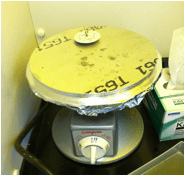
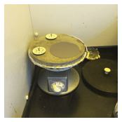
Baker set to 150°C
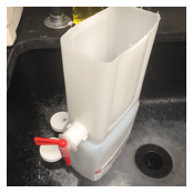
2. Setup a 40% by weight KOH 1 (or 2) liter bath in a large beaker on a hot plate set at 70°C for the later silicon etching step. Add a large magnetic stirrer to the KOH to reduce the temperature and salt gradient in the solution. Also, cover the beaker with Saran wrap in order to contain the evaporating KOH. Note: To make 40 % KOH, measure out 533 grams of KOH pellets into 800 ml of water (double these quantities for larger bath).
KOH bath set to 70°C
3. Piranha the thin region mask in a glass bath along with wafer under the acid/base hood at 250°C. Ensure that the chromium side of the mask is facing upwards and the piranha [1:2 hydrogen peroxide: sulfuric acid] covers the entirety of both surfaces. Keep in the piranha solution for 5 minutes, while agitating the bath to ensure proper cleaning. Flip wafer in bath at half way time point. Do not flip the mask.
4. Carefully remove mask from bath and place in ddH2O bath using a plastic tub open at the top, with a spigot at the bottom. After 7x water volume has filled the bath, remove the mask by gently gripping the edges and dry using N2 gun.
Mask drying with N2 gun
5. Repeat step 4 with the wafer, using the ddH2O bath pictured below.

Wafer ddH2O bath
6. Prepare two plastic lids in the organic hood, one filled with developer solution, and the other with ddH2O. Ensure the lids are labeled. They will be used later in the procedure.
7. Place the wafer on the center of the spin-coater and press VACUUM to suction the wafer to the spinner. Ensure that the yellow vacuum knob to the right of the hood is loosened and press the wafer on the edges with tweezers to confirm that the vacuum is active.

Wafer on vacuum Vacuum and spin settings
8. Spin the wafer first without photoresist to see how well centered and balanced it is. Do this by pressing START. To manually stop the spinning at any point press RESET. If adjustments to the wafer positioning need to be made press VACUUM make the appropriate adjustments, and then press VACUUM again to secure the wafer.
9. Once the wafer is in the desired position, clean the surface by pressing START, allow the wafer to begin spinning at a moderate speed, and then spray isopropanol on the wafer while it’s spinning. Allow the wafer to dry and then stop the spinner by pressing RESET.
10. Apply 2.5 mL of photoresist to the center of the wafer using a large plastic pipette.

Wafer with photoresist
11. Press START to begin spin-coating the wafer with photoresist at 4500 RPM for 50 seconds (it will stop at 50 seconds automatically).
12. Check to see that the photoresist is applying uniformly across the entire surface and that there are no damages to the coat. If necessary, repeat this starting and stopping process of the spinning until you ensure that resist is applied completely across the surface.
13. Once the spin-coating is complete, press RESET then VACUUM to release the wafer from the vacuum. Place and bake the wafer on the baker at 125°C for 2 minutes and 10 seconds exactly. Be careful to start the timer the moment that the wafer is placed on the hot plate.
Wafer on baker
14. Using the wafer tweezers, remove the wafer from the hot plate and place on the center of the mask aligner. Position the wafer so that the flat edge is aligned with the holder edge which is closest to the user. Once positioned in this manner, apply the vacuum by connecting the setup to vacuum and switching it on.


Lithography Apparatus Mask aligner
15. Use the N2 gun to clean the surface of the wafer from any dust particles.
16. Remove the piranha cleaned mask from the holder, holding it at the edges, and place it chrome side down with the writing to the right, into the mask aligner. It should click into place. Slide the four clips at the corners onto the mask to secure it into place and tighten the screws by hand.
17. Rotate the stage clockwise in order to raise the wafer up to the mask. Only rotate until the mask has moved up ¼ of the way. Do not over turn, or there could result in damage to the wafer.
Placing the Mask
18. Use the N2 gun to dispel any dust particles settled on the mask, and then insert the N2 gun into the rubber tubing. This will create positive pressure below the wafer, which will improve surface contact between the wafer and the mask.
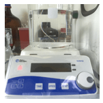
19. Clip the leads from the timer box to the LED array that is already hanging above the exposure apparatus. On the timer box, set the exposure time to what is desired (currently 29 seconds seems optimal) and turn the timer box and power supply connected to it ON.

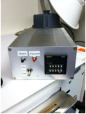
UV timer Power source
20. Center the LED array above the wafer/mask combination and press START on the timer box to begin UV exposure. DO NOT LOOK AT THE UV LIGHT, LOOK AWAY FOR THE 29 SECONDS.
21. Once exposure is complete, remove the nitrogen gas from the rubber tube to remove the positive pressure, turn off the vacuum, and move the stage down until it’s no longer making contact with the mask (counter-clockwise turning, about 10 turns). Remove the clips from the mask, and carefully lift the mask off of the holder (still holding it by the edges). Place the mask carefully back into its case.
22. Carry the wafer using the wafer tweezers to the organics hood, and submerge in the developer lid for about 45 seconds. Be sure to agitate the wafer by shaking and rotating the wafer constantly.
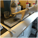
Developer solution
23. After the development fluid is done, move the wafer to the ddH2O lid as a primary water rinse, after which wash under the ddH2O tap in the sink and dry with the N2 gun.
24. To check for the thin regions, place the wafer under the microscope and focus on the area of the wafer that appears fuzzy (as seen below). The image should appear as a grid of small circles. Another test is how well the light from the microscope reflects on the wafer. If the light is 100% reflected then there are developed thin regions, and if the light is absorbed then the mask was ineffective on that part of the wafer. If the thin regions are not visible, wash the wafer with acetone to remove the photoresist and attempt steps 7-23 again.

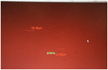
Wafer with thin regions Wafer under microscope Thin regions under microscope
25. ENSURE THE WAFER IS DRY (N2 gun) BEFORE PLACING IN THE RIE. Next, using the wafer tweezers, gently deposit the wafer inside the RIE. After 5 minutes vacuuming down, RIE the wafer for 60 seconds with SF6.
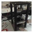
RIE
26. Repeat steps 7-25 for the other side of the wafer, with the chip outline mask.
Notes for second mask alignment: When placing the wafer on the mask aligner ensure that the flat side of the wafer is facing the user. Use the xyz controls on the wafer stage so that you can visibly see that the wafer’s flat edge is lined up with the mask’s bottom edge.

Aligning with xyz controls
Notes for second development: Keep wafer in developer solution for 60 seconds, or until the mask’s imprint is extremely clear. There is no need for the microscope.
Notes for second RIE: Etch for 7 minutes with SF6.
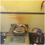
27. During the 7 minutes etch, prepare a BOE bath ¼ inch high in a rectangular plastic container and place it on the shaker in the acid/base hood.
28. If the wafer has an oxide layer: Spin coat the thin region side of the wafer using the dropper filled with photoresist. Place enough photoresist on the wafer to spread out 2 inches. After spin coating for 50 seconds, place on the 125°C baker for 2 minutes.
29. Etch the wafer in the BOE bath, with the visible mask side up (non thin region side) for 40 minutes. Turn on the shaker so the BOE bath is agitated gently. Be very cautious when handling the BOE since it does contain HF. This step will etch the silicon oxide that was exposed by our lithography. If the wafer has no oxide, skip to step 30.
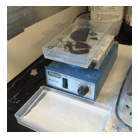
BOE bath on shaker
30. Rinse the wafer by placing it in an ddH2O bath for about 5 minutes.
31. To strip the wafer of the photoresist layers on both the top and bottom rinse it with acetone, followed by isopropanol, and then finish with drying the wafer with the N2 gun.
32. Place the wafer in a wafer holder and then place it into the KOH bath for an etching time of 16 hours. During this etch it is useful check that the solution is close to a temperature of ~70°C, which is optimal. It is also necessary to cover the beaker with Saran wrap during this etch to prevent the KOH from evaporating and diffusing out of the bath.
33. Wash the wafer after removing from KOH bath using the same water bath as was used for the mask in step 4 for 15 minutes.
ddH2O bath after KOH
34. To determine when the etching is complete, shine a light from the front to the backside of the wafer. When you can visibly see white light coming through the wafer where membranes are supposed to be present, the etching is complete. It may be necessary to remove the wafer from the solution to determine if light can be seen through the wafer. When doing this it is important to rinse the wafer first by placing it in a beaker of water and running water over it before viewing with the flashlight. This is to prevent KOH from drying onto the wafer surface. To avoid an over-etching, it is useful to check the membranes every 30-60 minutes with a flashlight to see if the etching is complete. When etching is complete, rinse the wafer with water to stop the silicon etch.
35. If the wafer has an oxide layer: To remove the silicon oxide layer exposed by the KOH, first clean the wafer using oxygen plasma in the RIE, for 30 second exposure, and then submerge and agitate in a ddH2O water bath to ensure the crater will be hydrophilic. Then etch by repeating steps 29 and 30.
36. If step 29 was done: Strip the wafer of the protective photoresist layer by rinsing with acetone, then isopropanol followed by drying with the N2 gun.
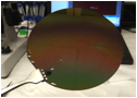
37. We now have a processed wafer of silicon nitride membranes ready for pore drilling or atomic layer deposition.
Processed wafer